Tuesday, November 28, 2023

Inside the Macintosh: the memory.

Let's start from this post with a series of posts with technical "dissection" of the different areas of the Macintosh mainboard. It's very important to understand how the hardware works.

Of course, a software emulator works differently from the real hardware, and many times it's a question of implementing tricks, especially when the emulator must run on a limited system such as a microcontroller.

So I will take my time in studying components, I will read the datasheets, and I will include also the link to download them.

I usually consider the memory of the computer first. ROM and RAM are absolutely necessary so let's take a look at the motherboard.

The amount of RAM present in the Macintosh 128K is... 128KB!!! WOW, what a surprise. The amount of ROM in total is 64KB. The ROM is made of two 32KB modules, together they make a 16-bit 32K words memory bank.

The geometry of the RAM instead is different. There are sixteen modules of 64K bits of dynamic RAM. These modules store a matrix of one column by 64K rows of single bits. Eight of these modules are addressed together to store a single byte, one bit for each module. Like the ROM there are two blocks of eight modules, that together make a 16-bit 64K words memory bank.


It's easy to understand how this RAM works. Take a look at the pinout of this module. 


Basically, the access to the internal storage happens in two main steps, keeping the line "WriteEnable" low for writing one bit, or high for reading one bit. These steps are needed to set the address of the bit in the range 16-bit wide. So RAS and CAS are asserted low to latch the high and low bytes of the address. According to the state of the WE line a bit is put on data pin Q (read), or the bit on data pin D (write) is written in the memory.

This access mechanism is not needed in a software emulator of course, but I am here to understand how this Mac works. But if you are interested in going deeper with access timings, here's the DRAM MT4264 datasheet.

In my emulator, this kind  of memory can be implemented easily with arrays, I think something like:  
uint16_t ram[65536];
const uint16_t rom[32768] = {
   /* Dump of the ROM */
};

But I will be back on the implementation later.

Sunday, November 19, 2023

An experiment just for fun.

I knew that "Digital" would enchant me. Especially for the fact that it gives me the opportunity to virtually replicate different areas of the Macintosh circuit to perform tests and understand how it works.

Now I would like to do an experiment. In truth, I don't need to go so low level for the emulator I have to write, but I'm curious to see how far this circuit simulator goes.

I want to try to implement the 64k-bit MT4264 DRAM memory chips present in the 128K Macintosh. So I found the datasheet, extracted the text of the description, and asked ChatGPT to synthesize the chip in Verilog naturally following the specifications.

What happened is interesting.

Hi, I want to build a DRAM module in Verilog. The DRAM size is 64k bits organized in 64k * 1. This is the description of the component in the datasheet. Can you write the Verilog module for me?

"The MT4264 is a randomly accessed solid-state memory containing 65,536 bits organized in a x1 configuration. During READ or WRITE cycles, each bit is uniquely ad- dressed through the 16 address bits, which are entered 8 bits (A0-A7) at a time. RAS is used to latch the first 8 bits and CAS the latter 8 bits. A READ or WRITE cycle is selected with the WE input. A logic HIGH on WE dictates READ mode while a logic LOW on WE dictates WRITE mode. During a WRITE cycle, data in (D) is latched by the falling edge of WE or CAS, whichever occurs last. If WE goes LOW prior to CAS going LOW, the output pin(s) remain open (High-Z) until the next CAS cycle. If WE goes LOW after data reaches the output pin(s), data out (Q) is activated and retains the selected cell data as long as CAS remains LOW (regardless of WE or RAS). This late WE pulse results in a READ-WRITE cycle. PAGE MODE operations allow faster data operations (READ, WRITE or READ-MODIFY-WRITE) within a row address (A0-A7) defined page boundary. The PAGE MODE cycle is always initiated with a row address strobed-in by RAS followed by a column address strobed-in by CAS. CAS may be toggled-in by holding RAS LOW and strobing- in different column addresses, thus executing faster memory cycles. Returning RAS HIGH terminates the PAGE MODE operation. Returning RAS and CAS HIGH terminates a memory cycle and decreases chip current to a reduced standby level. Also, the chip is preconditioned for the next cycle during the RAS HIGH time. Memory cell data is retained in its correct state by maintaining power and executing any RAS cycle (READ, WRITE, RAS-ONLY or HIDDEN RE- FRESH) so that all 256 combinations of RAS addresses (A0- A7) are executed at least every 4ms, regardless of sequence"

Creating a Verilog module for a DRAM such as the MT4264 involves simulating the behavior of the DRAM as described in your datasheet. In this simulation, you'll model the address latching with RAS and CAS, the READ and WRITE operations controlled by the WE signal, the data input and output handling, PAGE MODE operations, and the necessary timing for refresh cycles.

Here's a basic structure for such a module. This code is a simplified representation and may need adjustments based on the specific requirements of your system, such as timing constraints and interface details.

module MT4264 (
    input wire clk,        // System clock
    input wire rst,        // System reset
    input wire [7:0] addr, // 8-bit address input
    input wire ras,        // Row Address Strobe
    input wire cas,        // Column Address Strobe
    input wire we,         // Write Enable
    inout wire data        // Data line (bidirectional)
);

    // Memory array
    reg [0:0] memory [0:65535];
    reg [15:0] full_address;
    reg data_out;
    wire data_in;

    // Bidirectional data line
    assign data = (!we && !cas) ? data_out : 1'bz;
    assign data_in = data;

    // Latching addresses
    always @(posedge clk or posedge rst) begin
        if (rst) begin
            full_address <= 16'd0;
        end else begin
            if (!ras) full_address[15:8] <= addr; // Latch row address
            if (!cas) full_address[7:0] <= addr;  // Latch column address
        end
    end

    // Read/Write operations
    always @(posedge clk) begin
        if (!cas && !we) begin
            // Write operation
            memory[full_address] <= data_in;
        end else if (!cas && we) begin
            // Read operation
            data_out <= memory[full_address];
        end
    end

    // Refresh logic (simplified)
    // In real applications, refresh logic must cycle through all row addresses
    // within the required refresh interval (e.g., every 4ms).

endmodule

This module covers the basic address latching with RAS and CAS, and the READ/WRITE operations based on the WE signal. The "memory" array represents the DRAM cells. The actual refresh logic and PAGE MODE operations are not implemented in this example and would need to be added based on your specific requirements.

Remember that this is a simplified model and may not accurately represent all nuances of the real DRAM behavior, especially with regard to timing constraints and electrical characteristics. It's suitable for simulation purposes but might need adjustments for use in real hardware or more detailed simulations.

The data signal is not bidirectional. Can you split it into signal D as input data, and Q as output data.

Certainly, splitting the data signal into separate input and output lines makes sense for clarity and alignment with typical DRAM module designs. Here's the revised Verilog module with "D" as the input data signal and "Q" as the output data signal:

module MT4264 (
    input wire clk,        // System clock
    input wire rst,        // System reset
    input wire [7:0] addr, // 8-bit address input
    input wire ras,        // Row Address Strobe
    input wire cas,        // Column Address Strobe
    input wire we,         // Write Enable
    input wire d,          // Data input
    output reg q           // Data output
);

    // Memory array
    reg [0:0] memory [0:65535];
    reg [15:0] full_address;

    // Latching addresses
    always @(posedge clk or posedge rst) begin
        if (rst) begin
            full_address <= 16'd0;
        end else begin
            if (!ras) full_address[15:8] <= addr; // Latch row address
            if (!cas) full_address[7:0] <= addr;  // Latch column address
        end
    end

    // Read/Write operations
    always @(posedge clk) begin
        if (!cas && !we) begin
            // Write operation
            memory[full_address] <= d;
        end else if (!cas && we) begin
            // Read operation
            q <= memory[full_address];
        end
    end

    // Initialize the output
    initial begin
        q = 1'b0;
    end

    // Refresh logic (simplified)
    // In real applications, refresh logic must cycle through all row addresses
    // within the required refresh interval (e.g., every 4ms).

endmodule

In this version, "D" is used to write data into the memory array during write operations, and "Q" is used to hold the data read from the memory array during read operations. This separation aligns better with the actual DRAM interface, where data input and output are typically on separate lines.

Again, keep in mind that this is a basic model intended for simulation purposes and does not include all aspects of a real DRAM, such as detailed timing behavior, PAGE MODE operations, and comprehensive refresh logic.

by the way, signals RAS, CAS and WE are active low.

Thank you for clarifying that RAS, CAS, and WE are active-low signals. In Verilog, this means we should treat these signals as being active or 'asserted' when they are at a logical low level ("0"). I'll modify the code to reflect this behavior:

module MT4264 (
    input wire clk,        // System clock
    input wire rst,        // System reset
    input wire [7:0] addr, // 8-bit address input
    input wire ras_n,      // Row Address Strobe (active low)
    input wire cas_n,      // Column Address Strobe (active low)
    input wire we_n,       // Write Enable (active low)
    input wire d,          // Data input
    output reg q           // Data output
);

    // Memory array
    reg [0:0] memory [0:65535];
    reg [15:0] full_address;

    // Latching addresses
    always @(posedge clk or posedge rst) begin
        if (rst) begin
            full_address <= 16'd0;
        end else begin
            if (ras_n == 1'b0) full_address[15:8] <= addr; // Latch row address
            if (cas_n == 1'b0) full_address[7:0] <= addr;  // Latch column address
        end
    end

    // Read/Write operations
    always @(posedge clk) begin
        if (cas_n == 1'b0 && we_n == 1'b0) begin
            // Write operation
            memory[full_address] <= d;
        end else if (cas_n == 1'b0 && we_n == 1'b1) begin
            // Read operation
            q <= memory[full_address];
        end
    end

    // Initialize the output-
    initial begin
        q = 1'b0;
    end

    // Refresh logic (simplified)
    // In real applications, refresh logic must cycle through all row addresses
    // within the required refresh interval (e.g., every 4ms).

endmodule

In this revised module, "ras_n", "cas_n", and "we_n" are treated as active-low signals. The code checks for "0" (low) to determine when these signals are active. This approach better matches the behavior described in the datasheet and is common in hardware design where active-low control signals are used.

Remember, this is still a basic simulation model. For practical hardware implementation, you'll need to consider the specific timing requirements and characteristics of the DRAM, which are not fully captured in this simple model.

Another thing, this DRAM is asynchronous so the clock signal is not necessary.

You're absolutely correct. Asynchronous DRAMs, like the one described in your datasheet, do not use a system clock signal for their operation. Their actions are controlled entirely by the RAS, CAS, and WE signals, along with the address inputs. I'll revise the Verilog module to reflect this asynchronous behavior:

module MT4264 (
    input wire rst,        // System reset
    input wire [7:0] addr, // 8-bit address input
    input wire ras_n,      // Row Address Strobe (active low)
    input wire cas_n,      // Column Address Strobe (active low)
    input wire we_n,       // Write Enable (active low)
    input wire d,          // Data input
    output reg q           // Data output
);

    // Memory array
    reg [0:0] memory [0:65535];
    reg [15:0] full_address;
    reg [7:0] row_address;
    reg [7:0] col_address;

    // Latching addresses on the falling edge of RAS and CAS
    always @(negedge ras_n or negedge cas_n) begin
        if (!ras_n) row_address <= addr; // Latch row address
        if (!cas_n) col_address <= addr; // Latch column address
    end

    // Combine row and column addresses
    always @(*) begin
        full_address = {row_address, col_address};
    end

    // Read/Write operations
    always @(*) begin
        if (!cas_n) begin
            if (!we_n) begin
                // Write operation
                memory[full_address] <= d;
            end else begin
                // Read operation
                q <= memory[full_address];
            end
        end
    end

    // Initialize the output
    initial begin
        q = 1'b0;
    end

    // Refresh logic (simplified)
    // In real applications, refresh logic must cycle through all row addresses
    // within the required refresh interval (e.g., every 4ms).

endmodule

In this version, the "clk" input has been removed, and the operations are triggered by changes in the RAS and CAS signals (specifically their falling edges, which is typical for active-low control signals in asynchronous memory modules).

Since there's no clock signal, the operations are now handled by combinational logic ("always @(*)"). However, do note that this might lead to more power consumption in simulation as changes to the address or control lines would immediately reflect in the logic.

As always, this module is a simplified model and does not include specific timing behavior, detailed PAGE MODE operations, or comprehensive refresh logic, which are important in a real-world implementation.

the last thing, the original component doesn't have the reset signal.

Understood. If the original DRAM component, such as the MT4264, does not include a reset signal, we should remove it from the Verilog module to accurately reflect its functionality. Here's the revised code without the reset signal:

module MT4264 (
    input wire [7:0] addr, // 8-bit address input
    input wire ras_n,      // Row Address Strobe (active low)
    input wire cas_n,      // Column Address Strobe (active low)
    input wire we_n,       // Write Enable (active low)
    input wire d,          // Data input
    output reg q           // Data output
);

    // Memory array
    reg [0:0] memory [0:65535];
    reg [7:0] row_address;
    reg [7:0] col_address;

    // Latching addresses on the falling edge of RAS and CAS
    always @(negedge ras_n or negedge cas_n) begin
        if (!ras_n) row_address <= addr; // Latch row address
        if (!cas_n) col_address <= addr; // Latch column address
    end

    // Combine row and column addresses
    always @(*) begin
        // Combine the latched row and column addresses to form the full address
        full_address = {row_address, col_address};
    end

    // Read/Write operations
    always @(*) begin
        if (!cas_n) begin
            if (!we_n) begin
                // Write operation
                memory[full_address] <= d;
            end else begin
                // Read operation
                q <= memory[full_address];
            end
        end
    end

    // Initialize the output
    initial begin
        q = 1'b0;
    end

    // Refresh logic (simplified)
    // In real applications, refresh logic must cycle through all row addresses
    // within the required refresh interval (e.g., every 4ms).

endmodule

In this version, the module no longer includes a "rst" (reset) input. The operations are controlled entirely by the address, RAS, CAS, and WE inputs. The memory is latched based on the state of the RAS and CAS signals, and read/write operations are performed accordingly.

Keep in mind that this is a basic model for simulation and conceptual understanding. Real-world DRAM behavior, especially concerning timing and refresh cycles, is more complex and would require additional logic and considerations in an accurate simulation or hardware implementation.

Uhm, I think you missed the full_address register

You're absolutely right. I apologize for that oversight. The "full_address" register is crucial for combining the row and column addresses. Let me correct that in the Verilog code:

module MT4264 (
    input wire [7:0] addr, // 8-bit address input
    input wire ras_n,      // Row Address Strobe (active low)
    input wire cas_n,      // Column Address Strobe (active low)
    input wire we_n,       // Write Enable (active low)
    input wire d,          // Data input
    output reg q           // Data output
);

    // Memory array
    reg [0:0] memory [0:65535];
    reg [7:0] row_address;
    reg [7:0] col_address;
    reg [15:0] full_address; // Combined row and column address

    // Latching addresses on the falling edge of RAS and CAS
    always @(negedge ras_n or negedge cas_n) begin
        if (!ras_n) row_address <= addr; // Latch row address
        if (!cas_n) col_address <= addr; // Latch column address
    end

    // Combine row and column addresses
    always @(*) begin
        full_address = {row_address, col_address};
    end

    // Read/Write operations
    always @(*) begin
        if (!cas_n) begin
            if (!we_n) begin
                // Write operation
                memory[full_address] <= d;
            end else begin
                // Read operation
                q <= memory[full_address];
            end
        end
    end

    // Initialize the output
    initial begin
        q = 1'b0;
    end

    // Refresh logic (simplified)
    // In real applications, refresh logic must cycle through all row addresses
    // within the required refresh interval (e.g., every 4ms).

endmodule

In this corrected version, "full_address" is correctly declared and used to combine the row and column addresses. This register is essential for addressing the correct memory cell within the 64K-bit array. Thank you for pointing out the mistake!

Remember that the A.I. it's not infallible, it's a risk to ask and copy/paste. The best intelligence is the one between the two ears!

Anyway, I tested the component in Verilog.

Unfortunately, by creating an array of 16 MT4264 DRAMs, the application struggles a bit in the initial compilation of the component. 

So, since it is not necessary at the moment, I will create two 64K*8bit memories using the native components which simulate a typical access of a dynamic RAM. 

Saturday, November 18, 2023

Bricks for this project, really?

I don't know if it's happened to you too, but when I study electronic diagrams it makes me want to "reconstruct" the circuit to see it work. It's as if your head starts to go faster in imagining that you already have all the components at hand, ready to be inserted into their respective sockets on the PCB.

It is also frustrating to note that the transition from a scheme to a prototype is not so immediate, especially in my current condition, where handling components, wires, and soldering iron has become a  little difficult. 

The "luck" is that I don't want to build such a complex prototype because I will use a development board on which an emulator will run.

Now I'm "only" studying how the components interact, so a digital electronic circuit simulator might be enough. But what do bricks have to do with it? Well, logic gates are the building blocks of computers, and having a tool that allows you to grow assemblies of logic gates and see them in action can be essential for reverse engineering.

After several days of searching, I found him, "Digital", fantastic. The author's page reads: "Digital is an easy-to-use digital logic designer and circuit simulator designed for educational purposes." Educational says. In my opinion, it is much, much more!


In addition to being simple and intuitive to use, it is very powerful and feature-rich. The thing I love is the ability to create custom components using VHDL or Verilog, but not only that, but you can also see them in action in the simulation. 

 But what struck me most? What if I say VGA? What? But of course, there is a component that is able to function as a VGA monitor, not in real time (yet) but manages to hook HSync, VSync, and RGB signals with pixel clocks available in many resolutions.


A fire lit up inside me, I forgot for a while my never-ending headache, and like a rocket I began to design the video circuit of the Macintosh, modifying the standard 640*480 VGA signal to display the resolution of 512*342, using only 16 pixels in repetition.

Crazy!

Needless to say, I will use it a lot, and I will reveal many surprises to you! Check this out!

https://github.com/hneemann/Digital

Monday, November 13, 2023

Diving deep in the Mac.

I've been diving online for days looking for technical information on the Apple Macintosh 128k hardware. In truth, I didn't find much, at least what I was looking for.

I was studying the diagrams and photos of the motherboard that I found, and I understood that the "custom" chips have a crucial role in the functioning of the Mac. 

They are called "PAL", or "Programmable Array Logic", and are programmed from the factory with particular programs that tell the chip how to configure the output signals based on the input signals.

They are used mostly to translate memory addresses into activation signals for specific components, this means that for example if I want to read bytes from the RAM, or from the serial port, the address of the access must stay in a specific range.                     

BMU0, BMU1, TSM, TSG, LAG, ASG are the names of the 6 wonders that do the hard work of communication between components and the CPU.

Let me ask ChatGPT if he knows something about them.

Tell me something about the PAL chips (BMU0, BMU1, TSM, TSG, LAG, ASG) that are in the Macintosh 128k.

The document "Inside Macintosh" provides some information about the PAL (Programmable Array Logic) chips used in the Macintosh 128K, but it does not offer a detailed explanation of each specific chip (BMU0, BMU1, TSM, TSG, LAG, ASG). These chips are part of the custom hardware design of the Macintosh 128K and play crucial roles in its operation. Here's a brief overview based on general knowledge:

1. BMU0 and BMU1 (Bus Management Unit 0 and 1): These chips are likely involved in managing data transfers across different buses within the computer system, such as between the CPU, memory, and I/O devices.

3. TSG (Timing Signal Generator): Similar to the TSM, the TSG would be involved in generating timing signals necessary for the operation of different parts of the computer, such as the CPU and memory.

4. LAG (Logic Array Generator): This chip might be used for generating specific logic functions required for the operation of the computer, possibly in relation to the CPU or memory management.

5. ASG (Analog Signal Generator): The ASG is mentioned in the context of the disk interface. It reads the disk speed buffer in RAM and generates voltages that control the disk speed. This is crucial for reading, writing, formatting, and ejecting disks.

These chips, being part of the custom hardware design of the Macintosh 128K, were specifically tailored to meet the unique requirements of the system, contributing to its efficiency and performance. For more detailed information about these chips, additional technical resources or hardware manuals specific to the Macintosh 128K would be required.

So, from the manual "Inside Macintosh" not that much, so I did some research, and I have sound some more information:


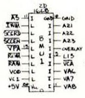
BMU1 is a 16L8 device that performs the major address decoding functions. 

It has as inputs the higher order address lines A21, A22, and A23 from the processor, along with the overlay bit (for a description of the overlay bit, see the August issue). 

These bits are decoded to generate enable signals for the RAM, ROM, IWM (disk controller), and the SCC serial chip.


LAG is a 16R8 device that performs the majority of the video control functions. 

It has as inputs most of the video address counter outputs, which are decoded to create output signals that load the video shift register, provide the CRT sweep circuitry with horizontal and vertical syncs, increment and reset the video address counters, and switch the RAM address multiplexers between CPU, video, and sound addresses.


BMU0 is a 16R4 device that generates RAM read and write signals from the RAM enable output of BMU1 and the processor R/W line. 

It is also used as a counter to create two video address lines (VA12 and VA13) because the video counter is only 12 bits wide (VA0-VA11). In addition, it also generates DTACK, the data transfer acknowledges the handshake signal to the processor and synchronizes the output of the video shift register with the master oscillator. 

 This is a very good example of the many different types of functions that can be handled with a single programmable device.


TSM is a 16R4 device whose major function is control of the dynamic RAM. For inputs, it has the decoded RAM enable signal, along with the address and data strobes from the processor which signify whether the data transfer will be low byte, high byte, or word. From these, the RAS and CAS strobes are generated, and the row/column address multiplexer is controlled. Until there were PALs, this type of dynamic RAM control function required either about 10-20 discrete TTL packages or a 40-pin LSI dynamic RAM controller which usually didn't do what you wanted anyway.


ASG is a 16R8 device which illustrates why PALs can be so valuable. Its primary purpose is to take the 6-bit disk speed value which is fetched at the end of every horizontal retrace period and convert it to a pulse-width modulated signal. Basically, it's a 6-bit counter. This leaves a couple of inputs and outputs available, which are used to control the loading of the sound generator pulse-width modulator, which is a counter made up of TTL devices. If a discrete counter had been used for the disk PWM, another chip would have been required for the sound PWM load function. Using a PAL for a simple counter function in this instance saved a chip in the design.


TSG is a 16R6 device that illustrates the power of programmable logic. It serves a couple of mundane functions concerning interrupts and the keyboard clock, but by far its most interesting job is as a clock generator for the SCC serial chip.

The master oscillator frequency in the Macintosh is 15.667 MHz. This is divided by 2 in the TSG to get the 7.834 MHz processor clock. In order for the SCC to be able to operate at a baud rate of 230.4 KBaud, which is what AppleTalk requires, it needs an input clock frequency of 3.686 MHz.

If you pull down your calculator desk accessory, you'll find that 15.667 ÷ 3.686 = 4.25. This means that the TSG needs to divide the 15.667 MHz master oscillator by 4.25 in order to get a 3.686 MHz clock. How is this done, since 4.25 is not even an integer, let alone a binary number?

Let's call the 15.667 MHz clock the MO_clk and the 3.686 MHz clock the SCC_clk. For every 17 MO_clk periods, there are 4 SCC_clk periods (17 ÷ 4 = 4.25). The way the TSG generates the SCC_clk is to count to 4 three times and then count to 5 once (4 + 4 + 4 + 5 = 17). See Figure 11 for a graphical description. Try that using a single TTL counter chip!

Monday, November 6, 2023

Know the hardware.

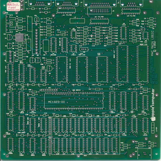
What we need also is a schematic of the mainboard of the Macintosh 128k, and a photo of the PCB, top and bottom side. 

I think that if I dig into the hardware I could learn more, and the development process should be a bit easier.

Unfortunately, ChatGPT can't help me find those on the Internet, so I did it by myself. It has been difficult to find them but in the end, I have found something useful.


Sunday, November 5, 2023

Where to start from.

Now that I've set an environment for the development of tests that I can share with you, I am going back to the emulator

My first idea is to design a main section based on a Finite State Machine, that is executed every cycle of the host application. In my Replit project this application is the SDL based environment, while in the STM32 board is a specific H7 targeted project.

I would like to develop this emulator as a scalable and portable application to have it running on different target platforms. My goal here is not to build a commercial product, but to learn, experiment and enjoy the development of an Apple Macintosh 128k.

There are different approaches in building an emulator. Usually, it should be best to start from a minimalist virtual system, so CPU, RAM, ROM, and the minimum hardware used to control the system. But it may not be fun. The systems that I have written a emulator were equipped with a Video Display Processor, so I started to write my emulators from the video stage. This let me to set a visual output system to be used to show debug information.

When I asked ChatGPT to give me information about the Apple Macintosh 128k, it provided me some details on the graphics section. I to was...

Good morning, thanks for this initial information. Now let's proceed in order. I would like a more detailed description of the hardware divided into areas.

And the answer for the graphics section was...

3. Display:

  • Tipo: CRT (tubo a raggi catodici) monocromatico incorporato
  • Dimensione: 9 pollici (diagonale)
  • Risoluzione: 512 x 342 pixel, il che offriva un'immagine sorprendentemente nitida e dettagliata per l'epoca, supportando l'interfaccia grafica dettagliata del Mac.

Actually not many details, Ineed to understand how graphics is generatedfor the video signal.

How graphics are generated on Apple Macintosh 128k?

The graphics on the Apple Macintosh 128K are generated through a combination of hardware and software components. Here's a basic description of the process:

1. Microprocessor: The Macintosh contains a Motorola MC68000 microprocessor, which is the central processing unit responsible for executing instructions, including those for graphic generation.

2. Video Display: The Macintosh uses a bit-mapped video display. This means that the screen is composed of a grid of pixels, where each pixel's state (on or off) is controlled by a corresponding bit in the computer's memory.

3. Video Memory: The video generator uses 21,888 bytes of RAM to create a bit-mapped video image that is 512 pixels wide by 342 pixels tall. Each bit in this memory range controls a single pixel: a 0 bit represents a white pixel, and a 1 bit represents a black pixel.

4. Screen Buffers: There are two main screen buffers in the memory from which the video circuitry reads information to create the screen display: the main buffer and the alternate buffer. The starting addresses of these buffers depend on the total memory available in the Macintosh.

5. Video Scanning Pattern: A full screen display consists of 342 horizontal scan lines. The video scanning pattern includes a vertical blanking interval, which is the time taken by the electron beam to move from the last line of one frame to the first line of the next frame.

6. Toolbox and Operating System Routines: To maintain software compatibility across the Macintosh line and to allow for future changes to the hardware, developers are strongly advised to use the Toolbox and Operating System routines wherever possible for graphics generation.

7. Memory Addresses and Screen Size: It's important to note that memory addresses and screen size may differ across different Macintosh models. Therefore, developers should retrieve the video base address and bit mappings directly from the system to ensure compatibility.

The graphics generation process is designed to be flexible and to provide a high degree of control to the software, allowing for the creation of rich graphical user interfaces and applications that were a hallmark of the early Macintosh computers.

From this it seems that the CPU is responsible for drawing the graphics on the video frame buffer. When a screen has been drawn, somehow the CPU Enables the transfer of data to VIDEO through specific circuits respecting the timings of the video signal. There doesn't appear to be a GPU or VDP.

This could make your job of implementing video output much easier.

Thursday, November 2, 2023

Code sharing, such a great idea.

Difficulties can't stop me, maybe they delay my results but my strong will helps me to find out a way to get things done.

I had to stop for a couple of days, I had to go through several things, but I got an idea for this blog, and some enthusiasm made me get back on this track.

What if I can show you the working source code or the entire emulator? Wouldn't it be great to show directly inside a post a working part of the code? That's a real possibility with Replit.

For now, as an example, I opened a public Replit project where I will save demos shown here. Why Replit? I discovered that supports the use of the SDL library. That means GRAPHICS!! Moreover, it's possible to embed a project inside an <iframe> tag.

Check the "Code development" page!